[Jan Mrázek]’s success with 3D printing a solder paste stencil is awfully interesting, though he makes it clear that it is only a proof of concept. There are a lot of parts to this hack, so let’s step through them one at a time.
First of all, it turns out that converting a PCB solder paste layer into a 3D model is a bit of a challenge. A tool [Jan] found online didn’t work out, so he turned to OpenSCAD and wrote a script (available on GitHub) which takes two DXF files as input: one for the board outline, and one for the hole pattern. If you’re using KiCad, he has a Python script (also on GitHub) which will export the necessary data.
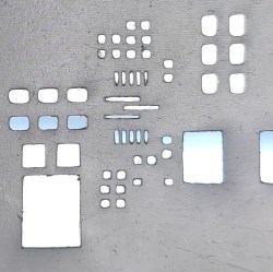
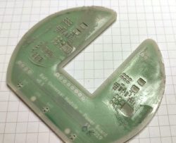
The result is a 3D model that is like a solder paste mask combined with a raised border to match the board outline, so that the whole thing self-aligns by fitting on top of the PCB. A handy feature, for sure. [Jan] says the model pictured here printed in less than 10 minutes. Workflow-wise, that certainly compares favorably to waiting for a stencil to arrive in the mail. But how do the actual solder-pasting results compare?

[Jan] says that the printed stencil had a few defects but it otherwise worked fine for 0.5 mm pitch ICs and 0402 resistors, and the fact that the 3D printed stencil self-registered onto the board was a welcome feature. That being said, it took a lot of work to get such results. [Jan]’s SLA printer is an Elegoo Mars, and he wasn’t able to have it create holes for 0.2 mm x 0.5 mm pads without first modifying his printer for better X/Y accuracy.
In the end, he admits that while a functional DIY solder stencil can be 3D printed in about 10 minutes, it’s not as though professionally-made stencils that give better results are particularly expensive or hard to get. Still, it’s a neat trick that could come in handy. Also, a quick reminder that we stepped through how to make a part in OpenSCAD in the past, which should help folks new to OpenSCAD make sense of [Jan]’s script.
No comments:
Post a Comment