If you were to travel back in time to the turn of the previous century and try to convince the average person that the grains of sand on just about any beach would be the basis of an industry worth hundreds of billions of dollars within 100 years, they’d probably have thought you were crazy. Aside from being coarse, rough, and irritating, sand is everywhere, and convincing anyone of its value would be a hard sell, unless your interlocutor was a real estate visionary with an appreciation of the future value of seaside property and a lot of patience.
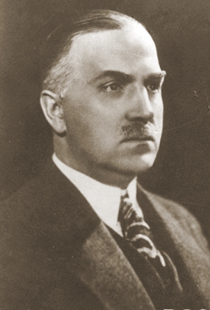
Fast forward to our time, and we all know the value of the material that comes from common quartz sand: silicon, specifically the ultra-purified crystals of silicon that end up as the wafers we depend on to build the circuitry of life. The trip from beach to chip foundry is a long and non-obvious one which would not have been possible without the insights of an undistinguished Polish student and one-time druggist who discovered the process that made the Information Age possible: Jan Czochralski.
Those Who Can’t Teach
Born in 1885 in what is now Kcynia, Poland but was then part of the Prussian Empire, Jan Czochralski showed an early aptitude for chemistry. As always seems the case with chemistry prodigies, an early experiment in his home laboratory resulted in an explosion. His father, a carpenter, had aspirations that Jan would one day become a teacher, but despite his love of chemistry, or perhaps because of it, Jan’s grades were poor enough to preclude him from that career path. As an alternative, he left home and took a job in a drug shop, vowing only to return to his hometown once he had become rich and famous.

Jan continued his studies on his own and progressed through a series of jobs in Germany’s burgeoning chemistry industry. He was largely self-trained when he applied to and was accepted by the Technische Hochschule in Berlin Charlottenburg, where he would specialize in metallurgy. Soon thereafter, as a newly minted chemical engineer at the Germany electrical giant AEG, he began studies into the applications in electronics of what was then an exotic and expensive material: aluminum.
Czochralski’s career was advancing rapidly on the value of his metallurgical research and the degree to which he published his findings. His work was cited frequently, so much so that he would one day become one of the most referenced Polish scientists, no mean feat when the list includes names like Marie Skłodowska Curie and Stanisław Ulam. His fame was eventually such that Henry Ford would court him aggressively and offer to put him in charge of his entire factory in 1923. Czochralski politely declined.
Absent-Minded Professor?
For someone who was so driven and devoted to the field of chemical metallurgy, and for as methodical as Czochralski reportedly was, it’s ironic that what he is perhaps best known for, and the discovery that would certainly become his most important legacy, was the result of an accident. In 1916, as the story goes, Czochralski was making some notes on a metallurgical experiment at his bench. Intent on his notebook pages, he didn’t notice that instead of dipping his pen into the inkwell, he had dipped it into a crucible of molten tin. The story may be apocryphal, given that the melting point of tin is 232 °C and it would be unlikely that a careful experimenter like Czochralski would be so cavalier with a pot of molten metal, but however the pen got into the tin, the result was interesting.
When he withdrew the pen, a fine whisker of tin was drawn up with it from the pool of molten metal. Curious as to the nature of the thread, Czochralski analyzed it and was surprised to find that it was a single crystal. He continued to experiment with the technique, replacing the pen nib with various capillary tubes, and adding seed crystals to provide nucleation sites for crystal formation. He was soon able to produce single crystals of various metals up to 1 mm in diameter and as long as a meter and a half. In addition to tin, he used his method to produce crystal filaments of lead and zinc.
Czochralski duly reported his findings in 1917, and though there was an initial burst of experimentation by others into the “Czochralski method”, the distractions of back-to-back world wars left the work largely in obscurity. He continued working in the chemical industry for the rest of his life, and would live long enough to see researchers at Bell Labs — it’s always Bell Labs — rediscover his process in the late 1940s and apply it to materials he never imagined working with, like silicon and germanium, as they began to invent the semiconductor industry.
Planting the Seed

The details of the Czochralski process for producing the single enormous silicon crystals, or boules, that are the raw material of almost every semiconductor product made today varies from the original method only in minor details, and of course in the scale of production. Silicon boule production is carried out in an induction furnace that has precise temperature control and can be provided with an inert atmosphere such as argon. The process starts when a quartz crucible is charged with ultrapure (99.9999%, or one non-silicon molecule in a million) polycrystalline silicon. The furnace is heated to about 1,500 °C while the crucible slowly rotates.
When the polysilicon has melted, a puller rod is lowered into the molten silicon pool. The end of the puller rod carries a seed crystal of silicon in a precise orientation, to serve as a nucleation site for crystallization. The puller rod, which is rotating in the opposite direction from the crucible, remains in the molten silicon for a short time before slowly being withdrawn. The molten silicon has by this point started to crystallize, and the puller rod begins accumulating a cone of crystalline silicon in the same orientation as the seed crystal.
Eventually the growing crystal reaches its maximum diameter, and the boule becomes more cylindrical. The diameter of the boule can reach up to 300 mm routinely, although 450 mm diameter processes are currently being prototyped; a theoretical maximum of 675 mm is possible but has not been attained. The boule continues to grow as it is withdrawn, a single crystal of silicon dangling from the puller rod and eventually weighing several hundred kilograms. The video above gives a good overview of the entire process, from production of polycrystalline silicon from quartzite sand through boule formation, and on to the fascinating details of processing the boule into wafers.
Not Just for Silicon Anymore

The Czochralski process is not only used for silicon crystals. Synthetic gemstones, including ruby, sapphire, garnet, and spinel can be grown using the method. On the other hand, the method is far from the only way of making ingots of monocrystalline silicon.
The float-zone process, also developed at Bell Labs, uses RF energy to heat a zone within a rod of polycrystalline silicon. It can produce silicon of much higher purity since the melt isn’t exposed to oxygen by the quartz crucible of the Czochralski method. There’s also the Bridgman–Stockbarger method, which is basically an upside-down version of the Czochralski method.
At the end of the day, though, Jan Czochralski’s accidental discovery of a crystal-growing technique has stood the test of time, as something like 90% of silicon wafers are cut from boules grown using his method.
No comments:
Post a Comment