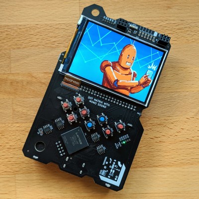
Kids of the 1990’s would call you a liar if you told them that within thirty years you’d go to a conference and be handed a Super Nintendo Entertainment System to wear around your neck. But that’s what happened with the badge Jeroen Domburg, aka [Sprite_TM], designed for the 2019 Hackaday Superconference. It’s built in the Game Boy form factor, complete with a cartridge slot, beautiful screen, and the familiar button layout. But there’s so much more here, like the HDMI port on the bottom and the ability to completely reconfigure the device by dropping a binary file onto it over USB.
Of course what makes this possible is the FPGA at the heart of the design. The story of how the badge was developed is shared in great detail during Sprite’s Supercon talk. The timeline, the hardware choices, and the oopses along the way make for a great story. But what you really don’t want to miss is how he built the machine inside of the FPGA — the collection of Verilog code known as “gateware” that brings together the System-on-a-Chip (SoC). From his delight at being able to spawn more processor cores by changing a single variable, to the fascinating SNES-inspired graphics subsystem, the inside story shared below is even more interesting than the physical device itself.
Hardware is Hard
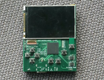
There’s a lot going on with this badge. On the PCB you’ll find a Lattice LFE5U-45F FPGA which comes in a 381 caBGA package with a whopping 203 available I/O signals. Imagine routing that on a PCB to connect up multiple RAM and Flash chips, the color LCD, 40-pin cartridge slot, IrDA, USB, HDMI, and multiple RGB LEDs. Now imagine doing it twice!
 One of Sprite’s biggest lessons on the hardware side of things is that you shouldn’t push the board house’s tolerances too hard. His prototype followed the design rules stated on the company’s website, but only some of the boards he got back actually worked. The failure rate was far too high, with actual production far from stated capabilities. The complete re-routing was to increase the minimum trace width which resulted in much better yields on the subsequent batch.
He shares a quick tip on prototyping; choose a different solder mask color for each prototype run and you’ll always know which version you have in your hand. In this project he went through green, red, and blue, before arriving on the black solder mask of the production badge.
Cores and Peripherals
 The problem with FPGA projects is that once you have the hardware assembled it doesn’t actually do anything. You need a bit stream — that gateware mentioned earlier — that tells the FPGA its purpose. This badge is as open source as you can possibly get and that includes the processor cores. A variant of the RISC-V core called PICORV32 was chosen as the best balance between functionality, size, and especially because it is written in Verilog to match the rest of the work on the SoC.
Of course the whole idea of the badge is for people to get under the hood and hack on the thing. The entire system can be compiled using open source tools developed over the last year or two. To aid in that, Sean Cross (aka Xobs) packed a no-dependency version of the tools suitable for cross-platform use. User applications to run on the RISC-V can be flashed to the badge as USB mass storage, and thanks to help from Sylvain Munaut, the entire SoC can be reflashed using Device Firmware Upgrade (DFU) over USB. The expansion cartridge itself has a bit of flash memory on it, and the FPGA will run the bitstream it finds on any inserted cartridge.
The thing is, despite a relatively fast clock on the FPGA itself, the PICORV32 core only runs at about 6 MHz. How are you going to push pretty pixels to the 480×320 display with that clock speed? The SNES answered that question with a clever graphics subsystem and those tricks are built into this badge.
Layered Graphics Makes a Slow Processor Seem Fast
Microcontrollers handle dense displays by upping the clock speed, but the better trick is to use hardware. Rather than processing all of those pixels you can lean on the hardware to move memory around, which is exactly how this display gets to be blazing fast. For anyone interested in graphics, the documentation of this particular subsystem is a must read (and must bookmark for future reference). Five layers are used, background, framebuffer, two tile layers, and a sprite layer.

The tile layers and sprite layer are the most interesting. They use tile maps, PNG or TGA images that store 256 16×16 square images of up to sixteen colors. Rather than copying each pixel out, the processor just gives an index number to the proper tile and tells the system which tile-sized slot to put it in on the tile layer, hardware handles the actual copying. But it gets better, the two tile layers can be moved in 1/64th of a pixel increments to animate them. While the tile layers are a grid of sixteen-pixel tile locations, the sprite layer allows you to draw tiles at any pixel location, and to scale those tiles.
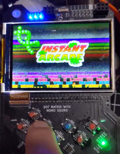
Sprite_TM discusses numerous other tricks built into the subsystem. You can rotate both sprite and tile layers, and he demonstrates an interesting color palette manipulation trick that gives the illusion of animating what is actually a static image. There’s even a register manipulation mechanism called The Copper which adds to the fun with wavy effects which you’ll recognize when you see them. A couple of weeks after Supercon, Bob Hickman posted up a demo on the badge that puts all of this to amazing use.
Too Much for One Person
Let’s be clear, the vast majority of the effort on this badge was put in my Sprite_TM himself. How he managed this over the course of only 10 months is a mystery. But many people jumped in to help get it across the finish line. A couple of dozen prototypes were made and put into the hands of people who volunteered to build up workshops around the badge, helping get people started on FPGA or to advancing the skills of those who had already given this field a try. Numerous people pitched in to hunt down bugs, build out subsystems like sound, improve the user experience though start screens and games, and to perform the final assembly.
I think I speak for everyone who got one of these badges in saying thank you all who helped make this happen, and especially to Jeroen Domburg. It’s undeniably impressive that this project came together in time for Supercon, and it represents an effort that may well never be topped. But at the same time it’s a testament to what happens when you combine a supremely-motivated hacker with a supportive community and superb open-source tools. This is a great world we live in.
Dig into the details of the FPGA badge on the Hackaday.io project page and the complete hardware and software repository.
No comments:
Post a Comment